Title : Prospective study of copper sulfide nanofilms
Abstract:
This keynote talk will be devoted to describe hexagonal Cu2S p-type semiconductor thin film fabrication using DC magnetron sputtering. Nanofilms with thickness gradient were successfully deposited by taking advantage of the deposition geometry and target dimensions. X-ray diffraction (XRD) analysis confirmed the exclusive formation of the hexagonal Cu2S phase. Elemental composition and thickness dependence with sample position were determined using energy-dispersive x-ray spectroscopy (EDS). Optical properties, including the optical bandgap and refractive index were assessed by modeling transmittance spectra. XRD data analysis successfully determined the film thickness as a function of sample position, aligning well with thickness values derived from transmittance spectra analyses. These results were further supported by film thickness values obtained from cross-sectional scanning electron microscopy (SEM) images. Charge carrier density and mobility, extracted from the optical models, were found to be consistent with DC electrical measurements.
Biography:
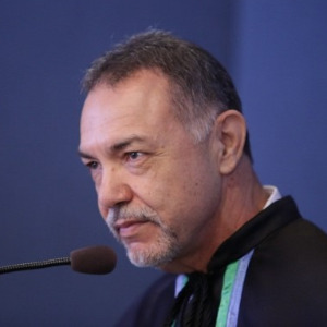
Paulo C. DE MORAIS (H-62), PhD, was full Professor of Physics at the University of Brasilia (UnB) – Brazil up to 2013, Appointed as UnB’s Emeritus Professor (2014), Appointed as Guest Professor of Huazhong University of Science and Technology – China (2011), Visiting Professor at Huazhong University of Science and Technology (HUST) – China (2012-2015), Appointed as Distinguished Professor at Anhui University (AHU) – China (2016-2019), Appointed as Full Professor at Catholic University of Brasília (UCB) – Brazil (2018), Appointed as CNPq-1A Research Fellowship since 2010. 2007 Master Research Prize from UnB, 2008-member of the European ERA NET Nanoscience Committee, Member of the IEEE-Magnetic Society Technical Committee, Senior Member of the IEEE Society, 2012 China’s 1000 Foreign Expert Recipient, and 2012 Academic Excellence Award from Brazilian Professor’s Union. He held two-years (1987-1988) post-doc position with Bell Communications Research – New Jersey, USA and received his Doctoral degree in Solid State Physics (1986) from the Federal University of Minas Gerais – Brazil. He graduated in both Chemistry (1976) and Physics (1977) at UnB. Professor Morais is member of the Brazilian Physical Society and the Institute of Electrical and Electronics Engineers – IEEE. He has served as referee for more than 50 technical journals, takes part of the Editorial Board of more than 15 technical journals and has conducted research on nanomaterials for over 40 years. He is known for his research in preparation, characterization and applications of nanosized materials (magnetic fluid, magnetoliposome, magnetic nanoemulsion, magnetic nanocapsule, magnetic nanofilm, magnetic nanocomposite, nanosized semiconductors, polymeric dots, carbon dots, and graphene quantum dots). With more than 500 published papers in peer reviewed journals, more than 14,500 citations, about 300 international invited talks (35 countries), and 16 filed patents. He has appeared in recent World ranking of top scientists, such as 2020-Stanford, 2022-Research.com, 2023-AD Scientific Index, 2023-Research.com, 2024-Elsevier, ONE Research Community, 2025-AD Scientific Index, 2025-Research.com, and 2025-Stanford-Elsevier.


